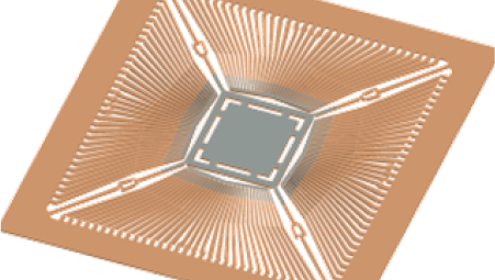
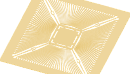
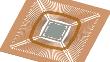
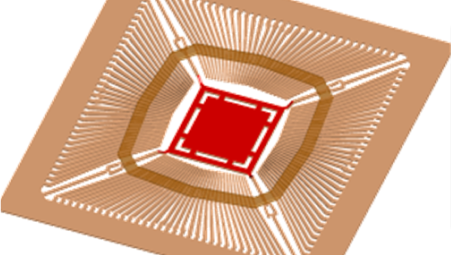
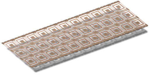
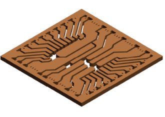
Lead Frame
Definition
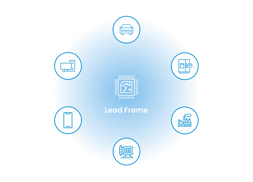
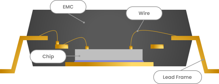
A lead frame is a key semiconductor component that electrically connectsa semiconductor chip to external circuits and serves as a substrate to support the chip within the semiconductor package.
Processes
Haesung DS implements various processes to deliver customized product designs for clients.
-
Etching / Stamping
-
Ag Plating
-
PPF Plating
-
Taping
-
Down-set
-
Down-set
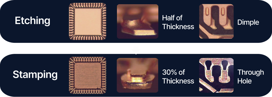
Etching
A chemical process that forms shapes through chemical treatments.
Stamping
A physical process that forms shapes using mold tools.
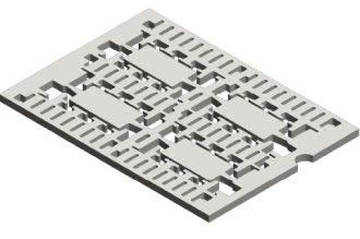
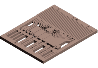
Product Types
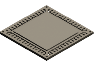
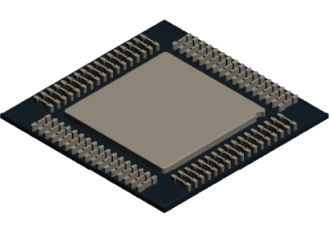
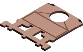
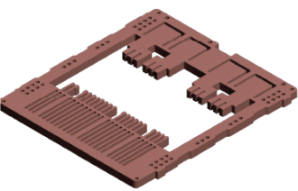
QFP (Quad Flat Package)
- A surface-mounted package with leads extending from all four sides.
- Supports a 110 μm inner lead pitch and exposed pad design.
Unit Design
-
lnner Lead Pitch 130μm
-
Power bar/Ground Ring
-
Locking Tape
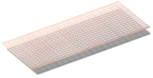
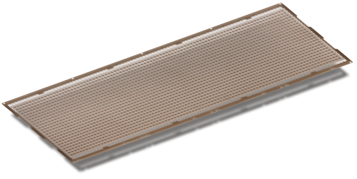
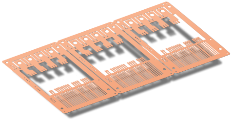
Strip Design
- Body Size(mm)
- 5~28
- Strip Size(mm)
- ~100 X 300
- Pin Count
- 32~216
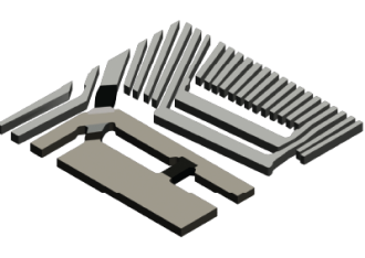
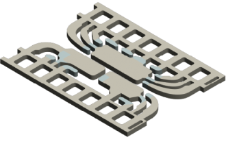
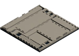
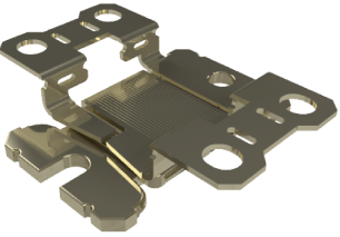
SOIC (Small Outline IC)
- A surface-mounted package with protruding leads extending from two sides
- Supports wide (100 x 300 mm) and high-density designs.
Unit Design
-
Inter Digit frame
(EX-Lead Sharing)

-
COL
-
Multi Pad
Strip Design
- Body Size(mm)
- 3~25
- Strip Size(mm)
- ~100 X 300
- Pin Count
- 6~56
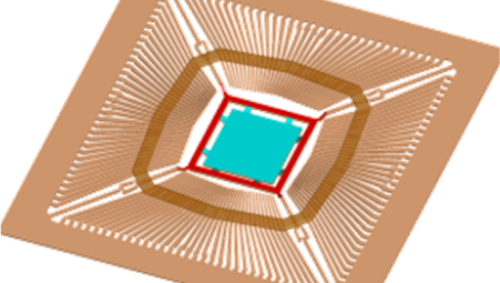
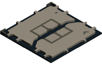
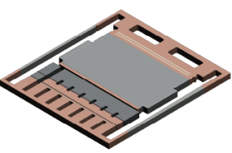
QFN (Quad Flat Non-lead)
- A package attached to the PCB without protruding leads.
- Supports dual land & flip chip configurations and implements a 130 μm wettable flank design
Unit Design
-
Single Row
-
Dual Row
-
Flip Chip
Strip Design
- Body Size(mm)
- 0.6~16
- Strip Size(mm)
- ~100 X 300
- Pin Count
- 4~180
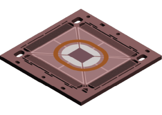
Rt-QFN (Routable QFN)
- A QFN package with a pre-mold application, offering high-design flexibility
- Enables precise pattern implementation and reduction of packaging processes
Unit Design
-
OFN Type
-
SiP Module Type
-
LED Type
Strip Design
- Body Size(mm)
- 2~15
- Strip Size(mm)
- ~78 X 290
- Pin Count
- ~160
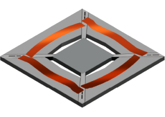
Discrete
- A single-function discrete package for high-speed / high-voltage power semiconductors.
- Supports implementation of non-standard raw material shapes and offers dual-side cooling solutions.
Unit Design
-
TO
-
TOLL
-
SOT-227
Strip Design
- Body Size(mm)
- 3~20
- Strip Size(mm)
- ~100 X 300
- Pin Count
- 1~6
Power Module
- A package attached to the PCB without protruding leads.
- Supports dual land & flip chip configurations and implements a 130 μm wettable flank design
Unit Design

-
Consumer
-
Automotive
-
Industry
Strip Design
- Body Size(mm)
- ~100
- Strip Size(mm)
- ~100 X 300
- Pin Count
- 1~6
Core Technology
High-precision punching tool technology
Offers high-design versatility and enhanced wire bonding efficiency.
Fine Punching
QFP : 110μm(Stamp), 150μm(Etch)
QFN : 180μm(Etch)
Precise Tooling
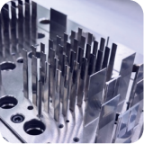
Tol. ±2μm / 1meter
Deep Down-Set Technology
Implements an exposed pad structure that facilitates efficient heat dissipation.
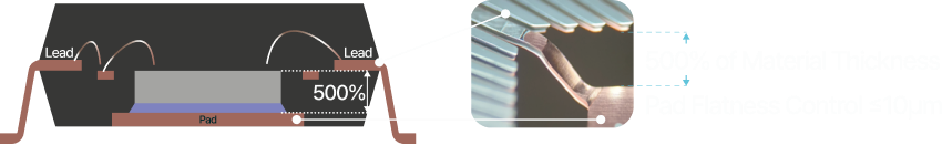
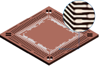
Deep Wettable Flank (130 μm)/h4>
Utilized for automated inspection of solder joints.
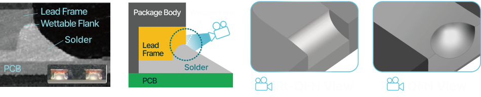
Implementation of Stamping Type QFN Configuration
Provides high productivity and cost competitiveness.
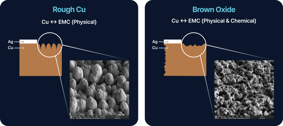
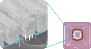
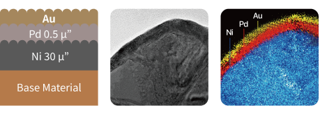
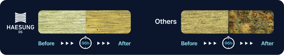
Surface Treatment Solution For High Reliability
- Enhances adhesion between EMC mold and lead frame through surface roughening techniques.
- Certified as a high-reliability solution for automotive use, meeting MSL Level 1 and AEC-Q100 Grade 0 standards.
μ-PPFTM
-
Passed TCoB with 6,000 cycles.
Forms a strong physical bond between EMC and lead frame through surface roughening treatment.
(Tested on LQFP 176 Pin / Temperature condition: -40~150Excellent corrosion resistance.
(Test conditions: Exposure to mixed flow gas for over 96 hours)
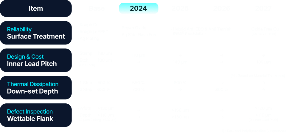
Technology RoadMap(~2027)

Application
High-Reliability Lead Frame Lineup for Automotive Semiconductors
Cu Roughening Technology